1 / 5
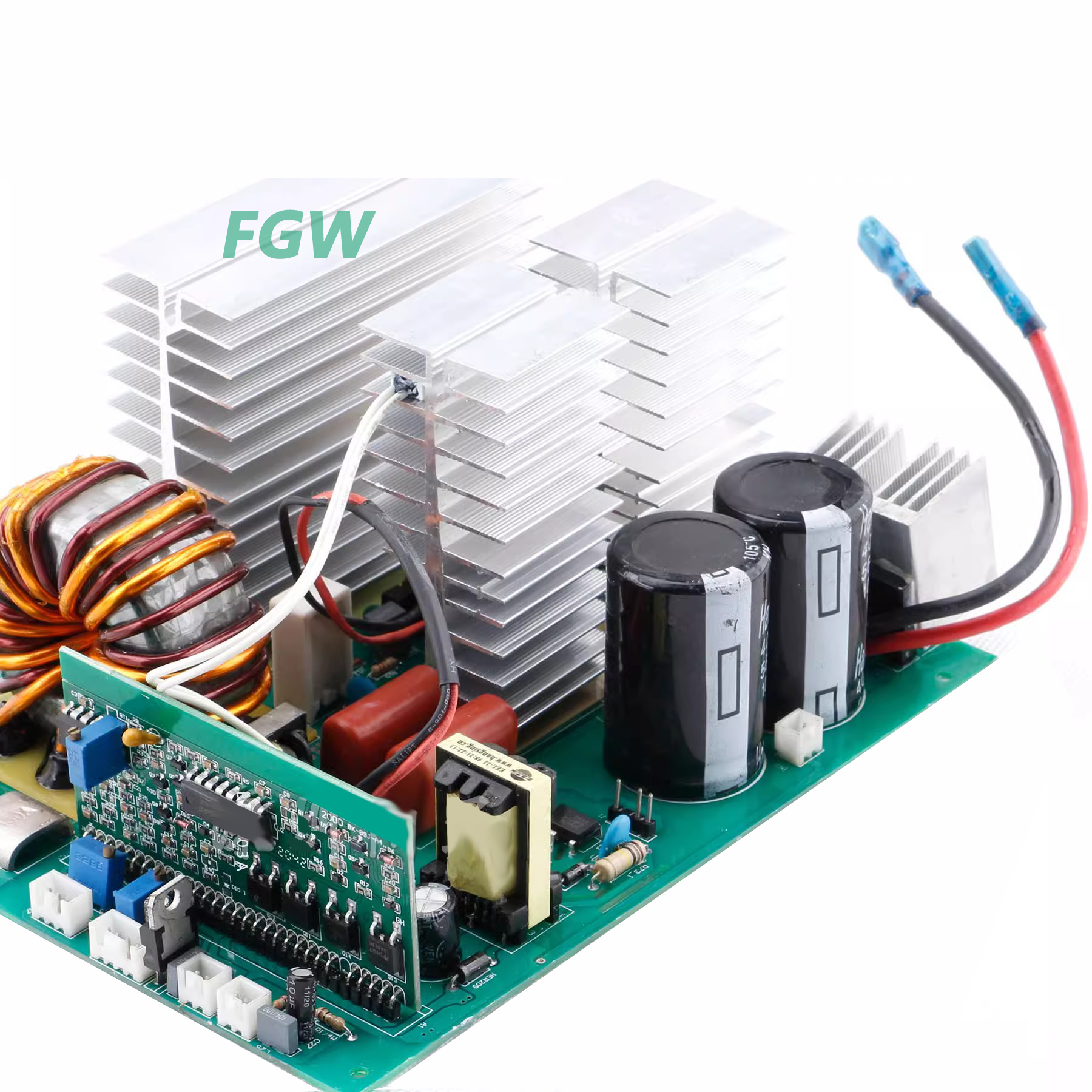
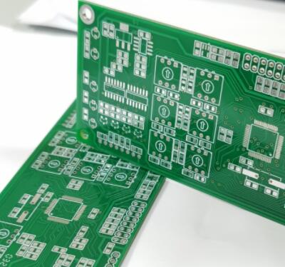
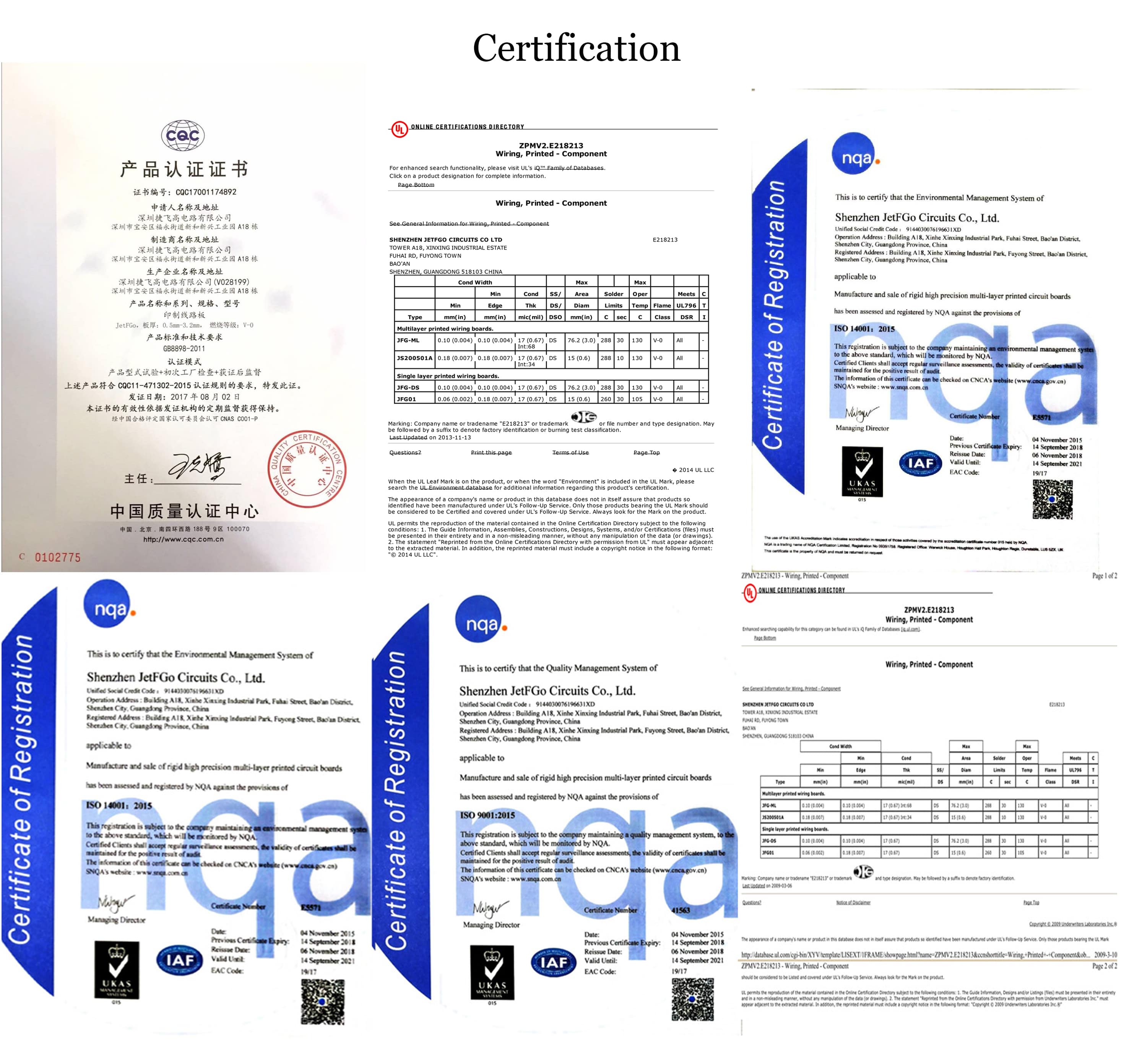
We are a leading manufacturer specializing in high-density multilayer printed circuit boards and specialty boards. With certifications including UL, ISO9001:2015, ISO14001:2015, CQC, IATF16949:2016, and "National Military Standard," we provide top-quality products and services. Our extensive product range includes multilayer boards, impedance boards, high-frequency boards, high TG thick copper foil boards, 5G high-speed boards, buried blind via boards, aluminum-based boards, hybrid dielectric boards, HDI, rigid-flex boards, specialty boards, and customized solutions.
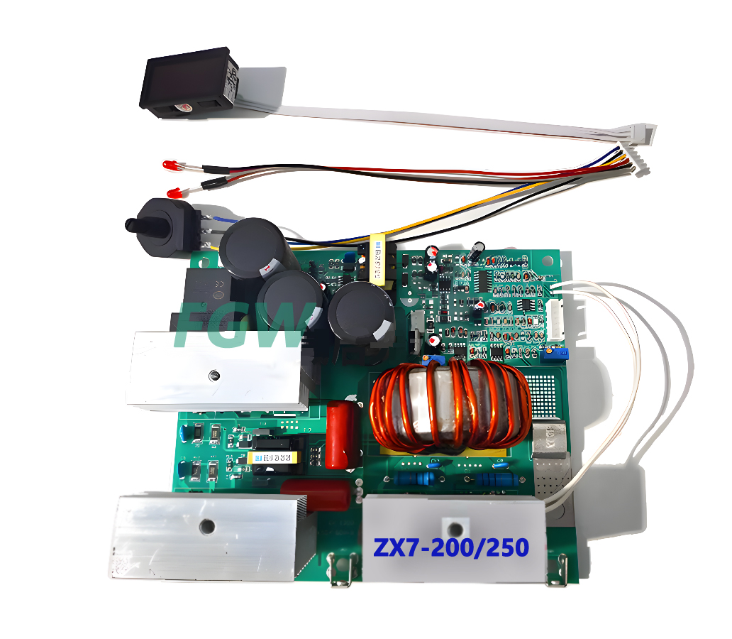
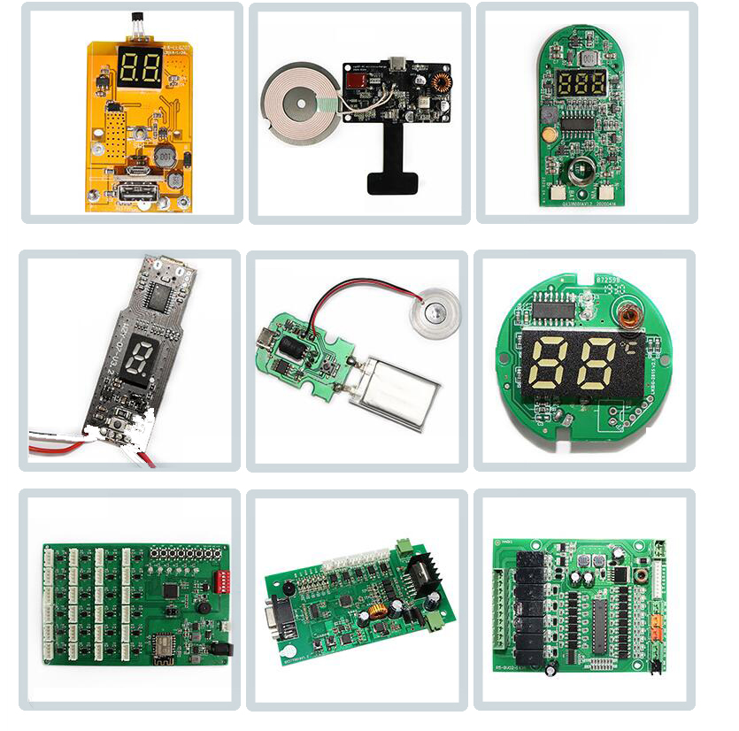
Driven by technological innovation, our products are widely used in industries such as communication equipment, industrial control, automotive electronics, energy and power, medical devices, IoT, research institutions, aerospace, and defense. With over 19 years of experience, we have served over 1,000 technology innovation-oriented enterprises with rapid prototyping and mass production services. We are committed to delivering cutting-edge solutions and exceeding customer expectations in the dynamic electronics industry.

Please note the following technical guidelines before purchasing:

| Rigid PCB Manufacturing Capability | ||
|---|---|---|
| Category | Volume Production | Sample Processing |
| Layer Count | 1-68L | 64 Layer |
| Max Thickness | 10mm (394mil) | 14mm (551mil) |
| Min Line Width / Space | ||
| Inner Layer | 2.2mil / 2.2mil | 2.0mil / 2.0mil |
| Outer Layer | 2.5mil / 2.5mil | 2.2mil / 2.2mil |
| Alignment Capability | ||
| Alignment with Core Board | ±25um | ±20um |
| Inner Layer Alignment | ±5mil | ±4mil |
| Max Copper | 6oz | 30oz |
| Hole Size Limit | ||
| Mechanical Drilling | ≥0.15mm (6mil) | ≥0.1mm (4mil) |
| Laser Drilling | 0.1mm (4mil) | 0.050mm (2mil) |
| Max Dimensions | ||
| Unit Size | 850mm x 570mm | 1000mm x 600mm |
| Panel Size | 1250mm x 570mm | 1320mm x 600mm |
| Aspect Ratio | ||
| Unit Aspect Ratio | 20:1 | 28:1 |
| Panel Aspect Ratio | 25:1 | 35:1 |
| Materials Used | ||
| Lead-Free / Halogen-Free | EM827, 370HR, S1000-2, IT180A, EM825, IT158, S1000 / S1155, R1566W, EM285, TU862HF | |
| High-Speed PCB Material | Megtron6, Megtron4, Megtron7, TU872SLK, FR408HR, N4000-13 Series, MW4000, MW2000, TU933 | |
| High-Frequency PCB Material | Ro3003, Ro3006, Ro4350B, Ro4360G2, Ro4835, CLTE, Genclad, RF35, FastRise27 | |
| Others | Polyimide, Tk, LCP, BT, C-ply, Fradflex, Omega, ZBC2000 | |
| Surface Finishes | HAL, HAL-LF, ENIG, Immersion Tin, OSP, Immersion Silver, Gold Finger, Hard Gold / Soft Gold Plating | |
| Special Technology | Blind & buried holes, Via in pad, Semi-plating holes, Counterbore, Step mounting holes, Drill Mixed RF PCB, Busbar PCB | |
Actual processing conditions are subject to final confirmation with support team.
As PCBs are custom products, returns are not supported. For verified quality issues, please contact support for a refund or replacement options. We do not bear any secondary losses or costs beyond the product value. Delays in delivery due to force majeure factors (such as power outages or water supply interruptions) will not be eligible for compensation.
For special instructions, please communicate directly with support for confirmation. Do not rely solely on system messages. Before and after payment, please confirm the process parameters, quantity, and layers. Claims made after production or shipment will not be eligible for refunds. Please consult with your technical engineers or our support team if ordering personnel lack the professional expertise.
Orders finalized before 17:00 are recorded as placed on the same day; orders after 17:00 are counted on the next day. "24-hour delivery" refers to one business day, not 24 consecutive hours. Delivery times provided do not include Sundays or official holidays.
Green solder mask, white silkscreen, 1.6mm board thickness, HASL surface finish, 1oz copper weight, vias tented with solder mask, minimum line width/spacing 0.2mm, vias diameter above 0.3mm. Gerber formats are processed based on the submitted layout files. Please inform support of any custom requirements for a revised quote.

We process PCB orders using the following logistic solutions:
| Layer Count | Sample Shortest Lead Time | Sample Standard Lead Time | Mass Production Lead Time |
|---|---|---|---|
| 2 Layer | 24 hours | 3 days | 6-7 days |
| 4 Layer | 36 hours | 5 days | 8-10 days |
| 6 Layer | 48 hours | 5 days | 8-12 days |
| 8 Layer | 72 hours | 5 days | 9-12 days |
| 10 Layer | 4 days | 7 days | 14 days |
| 12 Layer | 4 days | 7 days | 16 days |
| 14 Layer | 5 days | 8 days | 16 days |
| 16 Layer | 5 days | 9 days | 18 days |
| 18 Layer | 7 days | 10 days | 18 days |
| 20 Layer and Above | Negotiable | Negotiable | Negotiable |
We support high-frequency PCB materials including Ro3003, Ro3006, Ro4350B, Ro4360G2, Ro4835, CLTE, Genclad, RF35, and FastRise27. These are suitable for communication equipment, automotive radar, and high-frequency antenna projects.
Our shortest sample lead time is 24 hours for 2-layer PCBs, 36 hours for 4-layer PCBs, 48 hours for 6-layer PCBs, and 72 hours for 8-layer PCBs. Times are calculated from order confirmation, excluding Sundays and holidays.
Since PCBs are custom-made items, we do not support returns. We advise measuring the dimensions of your original boards and housing before ordering, and consulting with our technical support team to verify the installation layout.
We accept standard industry design formats including RS-274-X and RS-274-D Gerber files, DXP, Protel 99 SE, PADS, and GC-CAM files.
We can fabricate rigid PCBs up to 68 layers for volume orders, and 64 layers for prototype sample orders. The maximum copper thickness we support is 6oz for volume production and up to 30oz for specialized sample runs.
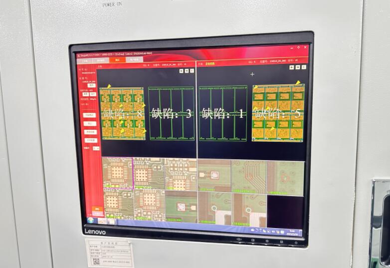
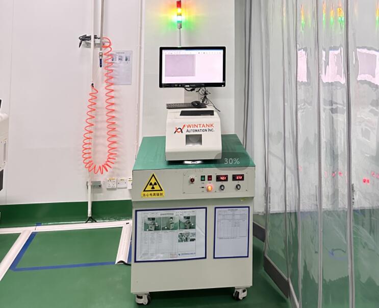
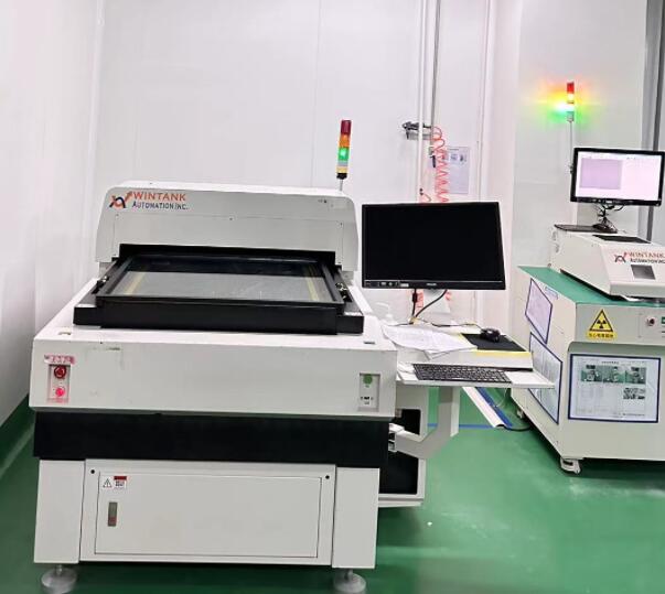
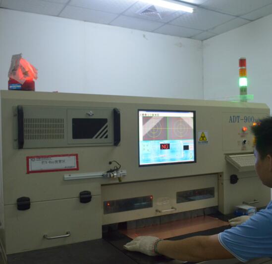
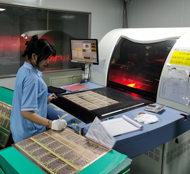
Our production adheres to ISO 9001, ISO 14001, IATF16949, RoHS, REACH, UL, and CQC quality standards. We conduct complete evaluations including metallographic microsections, electrical tests, and ionic contamination analysis to ensure all shipments meet IPC guidelines.