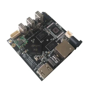
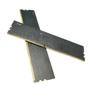
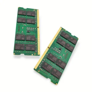
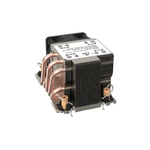
Explore our precision-engineered circuit modules, thermal control elements, and memory units designed to interface seamlessly with heavy copper power distribution networks.
In the domain of printed circuit board fabrication, Thick Copper PCBs—frequently categorized as Heavy Copper PCBs—are boards with copper weight structural designs exceeding 3 ounces per square foot (oz/ft²) in either their external or internal layer architectures. Standard PCBs typically deploy 1 oz/ft² (35 µm) or 2 oz/ft² (70 µm) of copper. Heavy copper architecture, conversely, scales anywhere from 3 oz/ft² (105 µm) up to 20 oz/ft² (700 µm), and in specialized extreme-power applications, even higher.
Thick copper increases the thermal conductivity of the board, allowing current-induced heat to diffuse outward rapidly to integrated metal cores or heatsinks.
Heavy copper paths easily carry elevated amperes without causing dielectric breakdown or excessive trace-temperature rises.
Enhanced plated through-hole (PTH) structures stand up to high thermal expansion cycles, mechanical shock, and localized high-temperature stress.
By utilizing specialized chemical deposition and advanced continuous electroplating techniques, we deposit thick, uniform copper matrices on standard FR4 substrates, metal cores, or high-reliability polyimide. The result is a robust power-delivery and control platform. Engineers in high-power sectors can consolidate multiple complex discrete wiring schemes into a single integrated board, reducing system envelope size, weight, and assembly defects.
Southern California, and particularly the Greater Los Angeles Metropolitan Area, acts as a primary global epicenter for technological research, aerospace engineering, defense, and clean technology. From aerospace clusters in El Segundo, Hawthorne, and Torrance to advanced electric vehicle (EV) developers in Orange County, local hardware designers demand extremely robust electronics built to survive harsh operating profiles.
Aerospace and Space Exploration: LA-based organizations designing spacecraft, satellites, and avionics systems require circuit configurations capable of operating reliably in vacuum environments where convection cooling is nonexistent. Thick copper PCBs satisfy this demand by conducting heat directly away from hot components via conduction.
Electric Vehicle (EV) Infrastructures: Southern California leads the nation in transitioning to zero-emission logistics. Heavy-duty fast chargers, high-voltage battery management systems (BMS), and motor inverters produced locally rely on multi-layer heavy copper substrates to manage up to 800V architectures and sustain heavy charging currents safely.
Globally, power grids are transforming. With the rapid expansion of hyperscale AI datacenters requiring massive high-current server racks, combined with the integration of renewable energy grids (solar inverter control, wind turbine yaw actuators, and industrial energy storage systems), the world faces an unprecedented need for reliable high-current power PCBs.
Procurement directors and hardware engineering teams in Los Angeles and global centers like Silicon Valley, Munich, Tokyo, and Seoul prioritize a handful of critical operational KPIs when selecting their export manufacturing partner:
While local design houses in Southern California drive high-level architecture, sourcing raw materials and scaling heavy-duty PCB manufacturing locally is often cost-prohibitive and slow. Chinese advanced PCB fabrication hubs provide the ideal operational counterweight.
By partnering with specialized manufacturers like Memvora Electronics Technology Co., Ltd., global hardware companies achieve optimal production yields. Our domestic supply chain integrations ensure immediate access to specialized high-Tg copper-clad laminates, robust chemistry for continuous electroplating lines, and automated LDI (Laser Direct Imaging) machinery optimized for deep, thick-layer profiles.
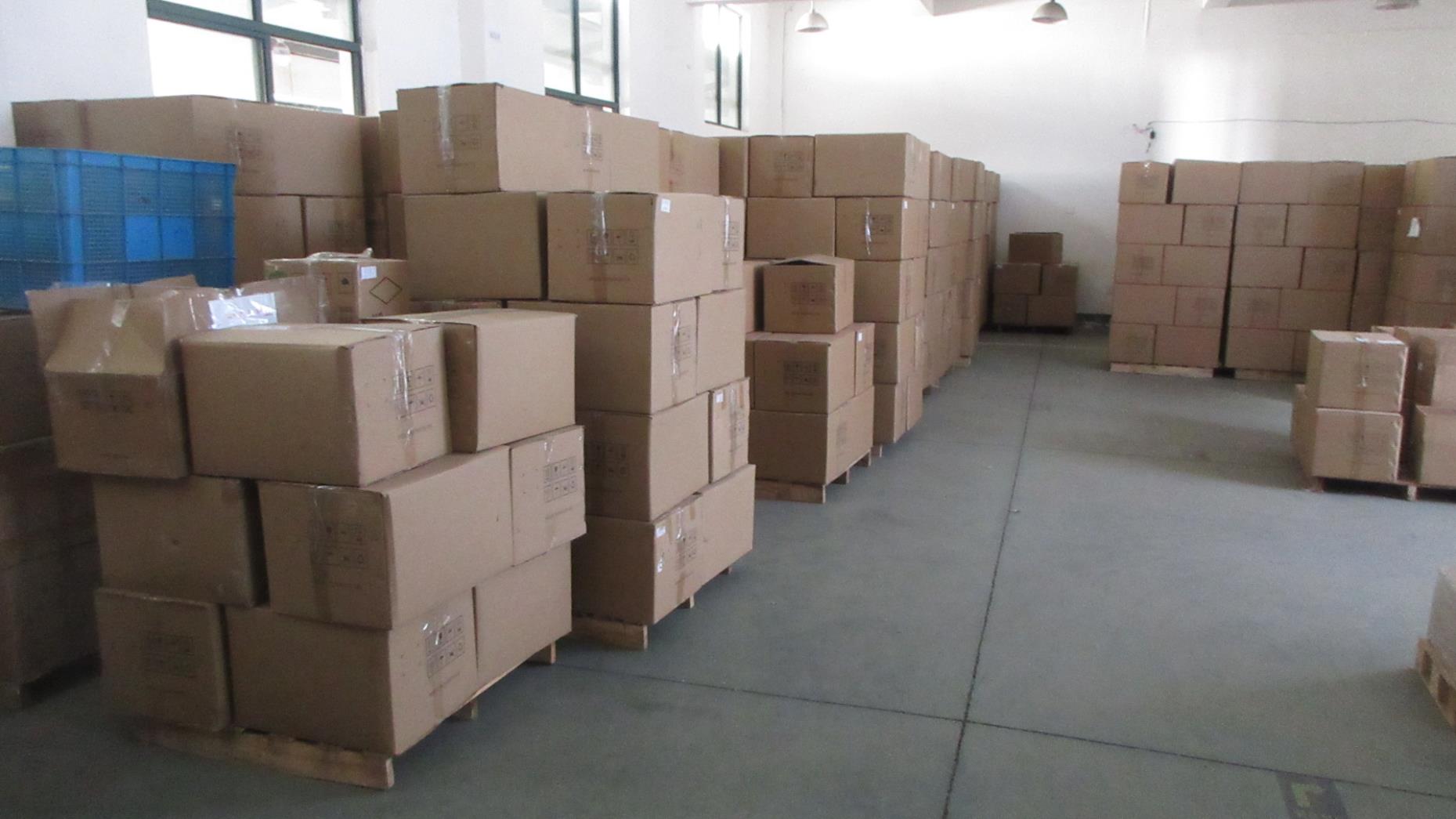
Furthermore, our highly streamlined logistics corridors routing through shipping terminals directly link our facilities to the Port of Los Angeles and LAX air cargo terminals, ensuring rapid transit. Standard thick copper PCB prototypes can be fabricated, tested, cleared, and delivered to California engineering tables within brief execution windows.
Engineering high-reliability thick copper PCBs requires meticulous attention to manufacturing limitations. Below are critical layout and fabrication design limits that engineers must consider during schematic capture and layout design:
As copper trace volumes increase, they influence the overall Coefficient of Thermal Expansion (CTE) of the composite board assembly. Copper expands at approximately 17 ppm/°C, while standard FR4 resin matrix packages expand at 14 to 16 ppm/°C on the X/Y axes, but significantly faster on the Z-axis (50–70 ppm/°C). Under thermal shock, this differential rate exerts significant stress on plated through-holes (PTH). Memvora resolves this by utilizing high-reliability substrates (High-Tg / High-Td FR4, polyimide) and thick, robust PTH barrel wall copper plating (minimum 1.2 mil / 30 µm thickness) to prevent corner cracking and barrel failure.
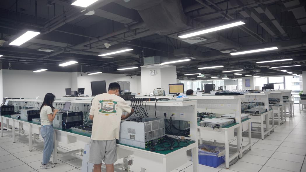
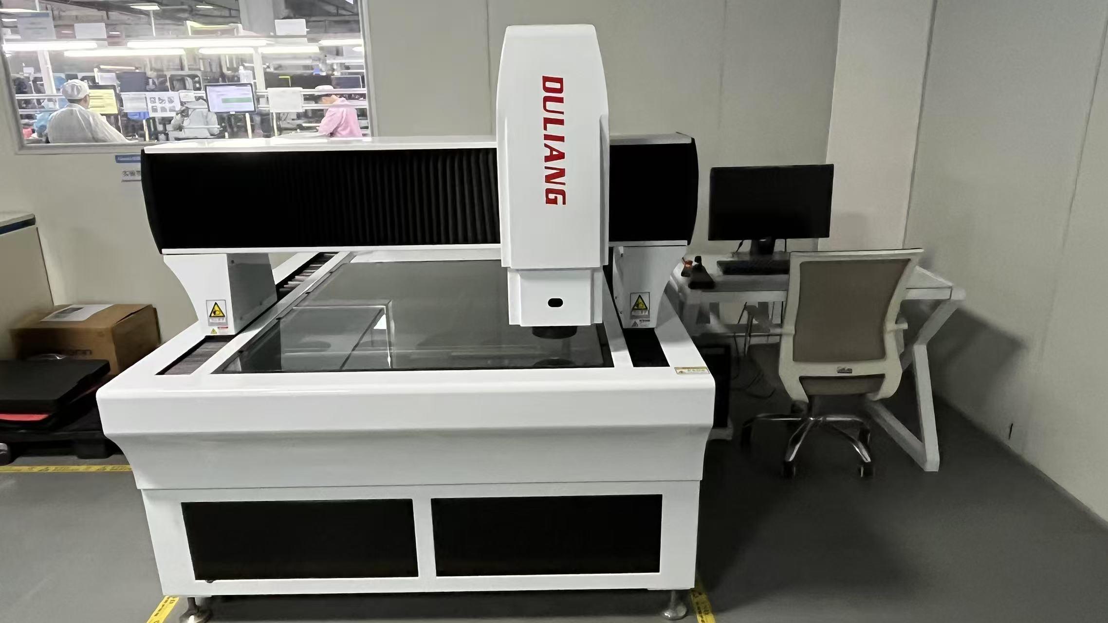
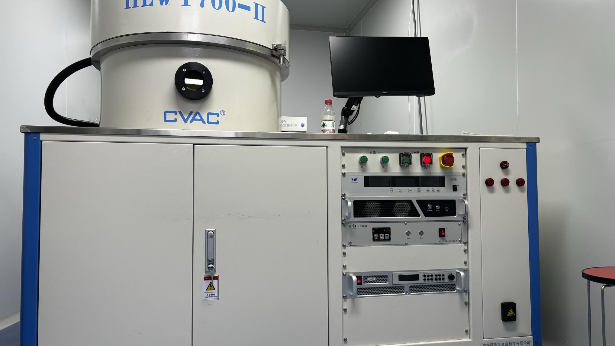
Founded in 2017, Memvora Electronics Technology Co., Ltd. is a professional manufacturer specializing in high-performance memory modules and advanced circuit assembly solutions. We are dedicated to delivering reliable memory, processing, and heavy-current hardware interfaces for consumer, industrial, enterprise, and embedded applications worldwide. With a modern engineering facility covering 386㎡, we combine advanced production equipment, strict quality management, and experienced engineering expertise to provide stable, high-speed hardware for global OEM and ODM partners.
Since entering the international market, Memvora has accumulated 7 years of export experience, serving customers across North America, Europe, Southeast Asia, the Middle East, and South America. Our annual export revenue exceeds US$18.6 million, supported by a strong global supply chain and long-term partnerships with more than 1,280 component suppliers and business partners.
With 14 years of industry experience, our team continuously invests in technology innovation and product development. Our R&D department consists of 126 professional engineers who focus on developing next-generation hardware designs with higher speed, lower latency, and enhanced reliability. Last year alone, we successfully launched 86 new products to meet the evolving needs of gaming, AI computing, industrial automation, and enterprise servers.
Quality is the foundation of everything we do. Every product undergoes 100% functional testing, burn-in testing, compatibility testing, signal integrity testing, and aging tests before shipment. Our dedicated quality control team of 42 inspectors ensures every memory module and circuit assembly meets rigorous international quality standards and delivers long-term stable performance.
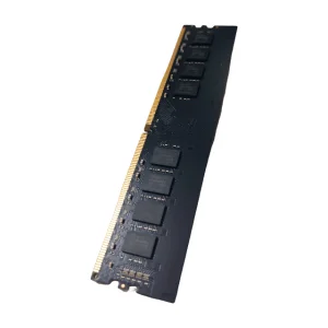
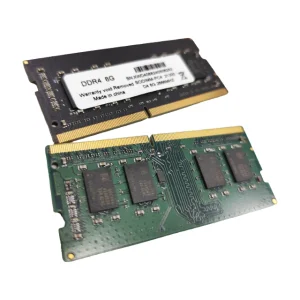
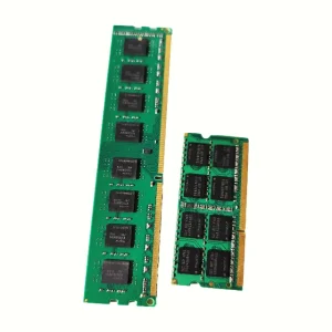
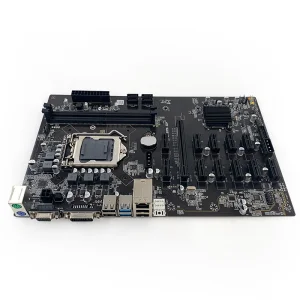
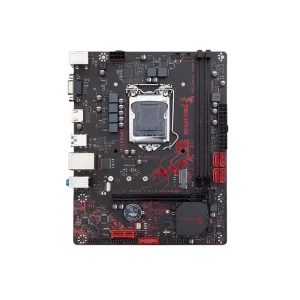
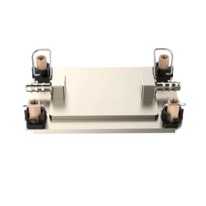
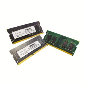
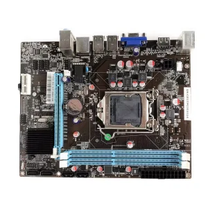
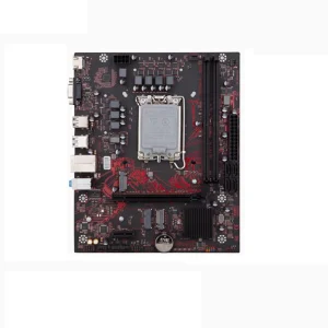
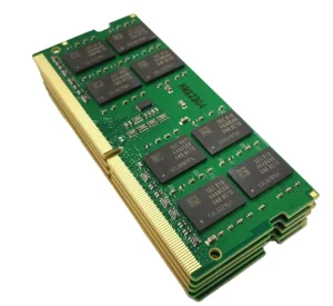
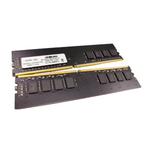
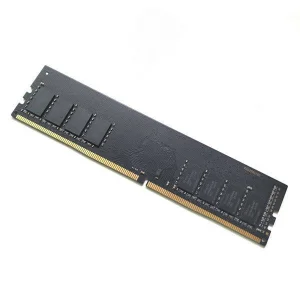
We provide the high-performance memory architectures, motherboard solutions, and CPU cooling technologies needed to interface with rugged, heavy copper backplanes and power circuits. Browse our catalog serving Los Angeles engineers:
Find direct answers to key technical, sourcing, and logistics questions concerning thick copper PCB manufacturing and export services to Los Angeles.
Whether you require early-stage prototype fabrication to test high-voltage systems or need bulk export capacity for industrial infrastructure deployments in Los Angeles, Memvora offers the engineering support you demand.
Send Inquiry Now