Luxembourg, the historic heart of European industry and logistics, is undergoing a profound digital transformation. With high-tech hubs in areas like Esch-sur-Alzette, Contern, and Lentzweiler, the Grand Duchy has pivoted towards smart manufacturing, advanced automotive components, space technology (Luxembourg Space Agency initiative), and aerospace defense electronics.
These high-reliability industries demand electronic components with zero defect margins. In the Surface Mount Technology (SMT) production line, the stencil is the single most critical factor determining paste print quality, which directly correlates with the overall yield of the printed circuit board assembly (PCBA). As the premier Laser Stencils Manufacturer & Exporter for Luxembourg, we engineer stencils that handle the challenges of complex component geometries, fine-pitch layouts, and heterogeneous assemblies.
For satellite and orbital telemetry systems assembled locally in Luxembourg, SMT solder connections must withstand extreme thermal cycling and high mechanical vibration. This requires perfectly uniform solder fillets. Our laser stencils utilize electro-polished apertures to achieve an Area Ratio of >0.66, ensuring consistent transfer efficiency of SAC305 and indium-alloy solder pastes.
Whether your production line is handling miniature sensor arrays for automotive safety systems (e.g., radar sensors and LiDAR systems) or complex multi-layer motherboards for industrial automation, our customized laser stencils provide the necessary dimensional stability and absolute aperture precision required for high-yield throughput.
Creating the ultimate laser stencil requires a synergy of high-grade raw materials and extreme-accuracy cutting technology. We utilize premium, stress-relieved SUS304 Fine Grain (FG) Stainless Steel foils. Fine Grain steel ensures that the micro-structure of the metal remains intact during the fast thermal cycles of the laser cut, preventing warping and micro-cracking along the aperture walls.
Our manufacturing facility utilizes advanced, German-engineered LPKF fiber-laser cutting systems. Traditional CO2 laser systems produce larger heat-affected zones (HAZ), which can deform small features (such as 01005 passives and 0.3mm pitch BGAs). Fiber laser cutting maintains a beam spot size of less than 20 microns, delivering precise, sharp corners and ideal trapezoidal aperture walls. The trapezoidal shape (wider on the board side than the squeegee side by 1 to 2 degrees) ensures optimal, friction-free release of the solder paste.
To meet the expectations of high-density interconnect (HDI) printed circuit boards, we provide specialized post-processing steps:
One of the biggest concerns for SMT assembly plants in Europe is lead time. A delay in receiving a corrected SMT stencil can stop a production line, costing thousands of Euros per hour. This is where the resilience of our Chinese manufacturing base combined with direct air networks to Luxembourg shines.
Operating in China’s premier electronics ecosystem allows us to stock a massive inventory of varying steel foil thicknesses (from 80µm to 300µm) and various frame tension sizes (e.g., DEK, ZelFlex, Vectorguard). Our engineering team runs on a 24/7 rotation. Once a CAD file (Gerber data) is received, our engineers review the aperture designs, perform DFM (Design for Manufacturing) analysis, adjust aspect/area ratios, and output to the laser machines within 2 hours.
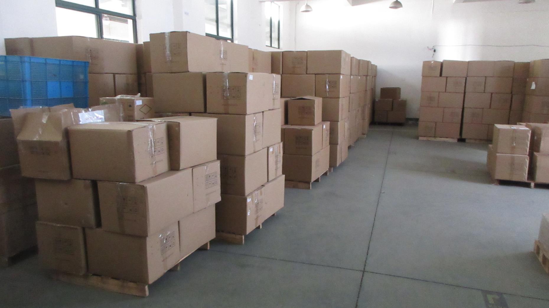
We utilize express air shipping partners (DHL, FedEx, UPS) and dedicated air cargo lines routing straight into Luxembourg Findel Airport (LUX), a key European logistics hub. Our stencils are packaged in custom-engineered, shock-absorbent wooden crates or double-wall corrugated boxes with inner high-density foam padding. This ensures stencils arrive with flat, unwarped frames and pristine foil tension. Standard delivery transit time from our factory floor to your SMT facility in Luxembourg is only 3 to 5 business days.
Moreover, our high manufacturing volume lets us leverage massive raw material procurement economies of scale. We pass these savings directly to our Luxembourg clients, offering high-precision, electro-polished, nano-coated laser stencils at a fraction of the cost of domestic European toolmakers, with comparable or even faster turnaround times.
The rapid ascent of AI hardware, 5G advanced modules, and automotive drive-train electronics (electric vehicles) is pushing component densities to unprecedented levels. Industry trends show the integration of 03015 and even 008004 chip passive components in multi-chip modules (MCM).
To support our clients in Luxembourg, our R&D department is actively executing our 2025–2030 technology roadmap:
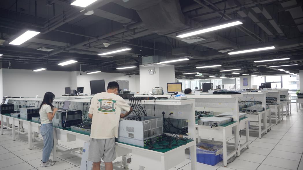
Founded in 2017, Memvora Electronics Technology Co., Ltd. is a professional manufacturer specializing in high-performance electronics infrastructure and micro-assembly tooling, dedicated to delivering reliable hardware and manufacturing solutions for consumer, industrial, enterprise, and embedded applications worldwide. With a modern manufacturing facility covering 386㎡, we combine advanced production equipment, strict quality management, and experienced engineering expertise to provide stable, high-speed memory products and high-precision laser stencils for global OEM and ODM partners.
Since entering the international market, Memvora has accumulated 7 years of export experience, serving customers across North America, Europe, Southeast Asia, the Middle East, and South America. Our strong global supply chain and long-term partnerships with more than 1,280 component suppliers and business partners enable us to provide consistent high-quality output.
With 14 years of industry experience, our team continuously invests in technology innovation and product development. Last year alone, we successfully launched 86 new hardware and SMT support products to meet the evolving needs of gaming, AI computing, industrial automation, and enterprise servers.
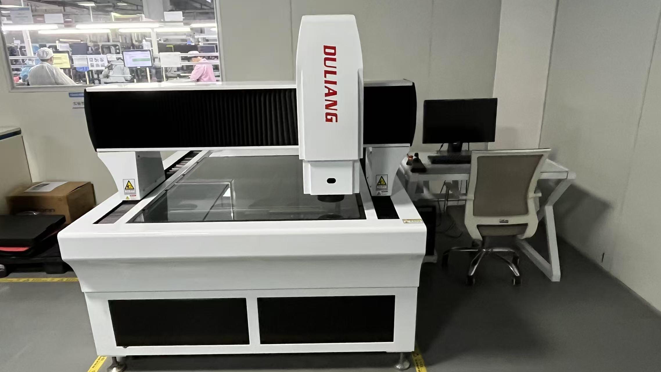
Quality is the foundation of everything we do. For our laser stencils, every sheet undergoes 100% Automatic Optical Inspection (AOI), tension testing, and microscopic aperture measurement before shipment. Our dedicated quality control team of 42 inspectors ensures every product meets rigorous international quality standards and delivers long-term stable performance on the production floor.
Memvora provides flexible OEM, ODM, private label, custom capacity, PCB color, heat spreader design, firmware optimization, and packaging customization services to meet different market requirements. Backed by a responsive engineering team and efficient production management, we help customers shorten development cycles and accelerate product launches.
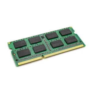
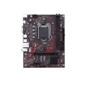
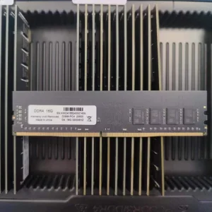
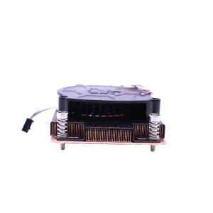
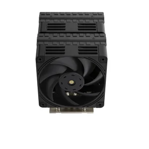
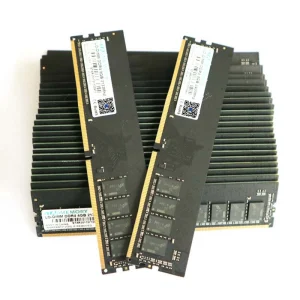
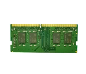
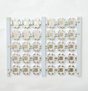
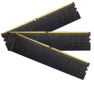
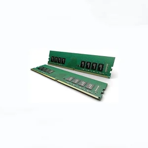
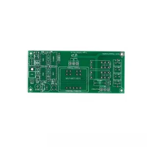
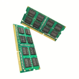
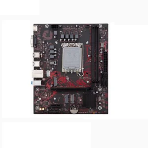
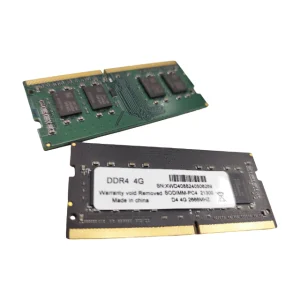
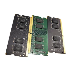
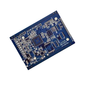
Below is our complete catalogue of high-speed SMT modules, system boards, heatsinks, and PCBs. All of these components rely on our custom-tailored laser stencil apertures to achieve optimal print quality and high industrial yield in Luxembourg manufacturing facilities.
As a leading exporter, we address the common technical and supply chain questions raised by manufacturing procurement teams in Luxembourg:
Partner with an experienced laser stencil manufacturer. Reduce your solder-related defects, speed up your production runs, and leverage cost-efficient, high-precision supply chains from China.
Send Inquiry Now