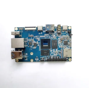
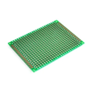
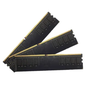
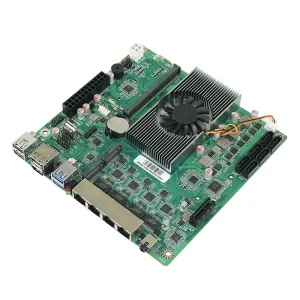
High-performance processing engines demand superior thermal stability. Discover our core catalog of heavy copper interfaces, motherboard units, and memory kits.
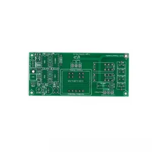
Modern electrical engineering is witnessing an unprecedented transition toward high-density power architectures. The proliferation of electric mobility, grid-scale renewable integrations, and artificial intelligence workloads has pushed traditional printed circuit board manufacturing beyond conventional boundaries. At the center of this transformation lies the demand for Thick Copper Circuit Boards (also referred to cross-industrially as Heavy Copper PCBs).
Unlike traditional printed boards which utilize standard copper weights of 0.5 oz/ft² to 2 oz/ft², thick copper configurations leverage copper trace layers exceeding 3 oz/ft² (105 µm) and scaling up to extreme designs exceeding 20 oz/ft² (700 µm). This massive increase in cross-sectional conduction area enables heavy copper architectures to accomplish three concurrent objectives: carrying extreme current loads, providing passive structural and thermal sinks directly inside the substrate, and significantly reducing localized ohmic losses (I²R losses) that jeopardize delicate silicon components.
To successfully implement heavy copper substrates in rugged operating environments, aerospace and automotive engineering designers must carefully calculate:
Heavy copper printed circuit board manufacturing acts as a key enabler for multi-billion dollar industrial markets globally. By substituting copper buss bars and external wiring harnesses with embedded thick traces, companies realize smaller product footprints and high manufacturing reliability.
Heavy duty power distribution systems, high-voltage motor control units, and grid transformers depend heavily on 4 oz to 10 oz copper layers. These structures reliably transmit hundreds of amps across switching elements without experiencing structural delamination due to high operating temperatures.
The transition toward 800V electric vehicle platforms requires robust onboard chargers (OBC), DC-DC converters, and battery management systems (BMS). Thick copper traces accommodate high voltage charging peaks while managing high thermal surges directly through the PCB dielectric.
In aerospace operations, wiring complexity introduces failure points and weight penalties. Heavy copper boards allow engineers to merge high-speed communication lines and high-current power distribution lines on a single unified multi-layer substrate, maintaining strict reliability under vibration and thermal cycles.
| Copper Weight (oz/ft²) | Copper Thickness (µm) | Recommended Trace Width (per 10A current) | Primary Industrial Applications |
|---|---|---|---|
| 3 oz | 105 µm | 3.5 mm (at 20°C Temp Rise) | Solar inverter switches, intermediate DC-DC converters, high-power audio amplifiers. |
| 5 oz | 175 µm | 2.1 mm (at 20°C Temp Rise) | EV battery management charging units (BMS), power distribution units (PDU). |
| 8 oz | 280 µm | 1.3 mm (at 20°C Temp Rise) | Military power supplies, heavy machinery controllers, electric vehicle drive trains. |
| 12+ oz | 420 µm+ | Under 1.0 mm (special design parameters) | Grid substation controllers, high-current busbar replacements, custom military applications. |
As silicon carbide (SiC) and gallium nitride (GaN) semiconductors scale, operating frequencies and temperatures are rising dramatically. The manufacturing technical roadmap for heavy copper must adapt to meet these demands.
Traditional subtractive chemical etching processes present challenges when handling thick copper. As copper thickness grows, lateral etching (undercutting) degrades trace profiles, resulting in inconsistent impedance values. Leading factories address this by utilizing advanced additive plating methodologies and specialized high-speed differential chemical spraying.
By deploying organic dry film photoresists designed specifically for thick-profile structures, fabricators achieve vertical sidewalls on copper traces, even up to 15 oz weights. This precision control allows for tighter trace spacing and higher wiring density on the board.
Thermal expansion differences between copper (CTE ~ 17 ppm/°C) and traditional FR4 fiberglass substrate (CTE ~ 14 ppm/°C in-plane, but significantly higher out-of-plane) present mechanical challenges. Extreme thermal stress testing is critical. Experienced heavy copper factories perform repeated thermal shock testing (spanning -55°C to +125°C for hundreds of cycles) and high-potency thermal stress tests (solder float tests at 288°C) to prevent inner-layer separation and delamination.
A primary challenge in multilayer heavy copper PCBs is ensuring that the prepreg resin completely fills the wide gaps between thick copper traces. Voids in these areas can lead to dielectric breakdown and field failures. The technical roadmap below outlines how advanced factories resolve these challenges:
Transitioning from standard FR4 to high glass transition temperature (Tg > 170°C to 180°C) and high decomposition temperature (Td) resins to withstand extreme assembly temperatures.
Utilizing high-flow epoxy resins combined with optimized vacuum press cycles to drive out microscopic air bubbles between thick traces.
Integrating heavy copper layers with aluminum or ceramic backplanes (insulated metal substrates) to maximize thermal dissipation in automotive charging hubs.
Understanding where heavy copper circuits are deployed locally helps clarify their value across modern industrial systems.
High-capacity solar inverter plants and local grid battery farms run continuous high currents. Heavy copper boards integrate control logic and high-power switches on the same board, eliminating interconnect resistance points that generate excess heat.
Subsea exploration equipment operates under extreme pressure and temperature cycles. Thick copper PCBs with robust cross-sectional tracks deliver stable power to robotic arms and sensor suites, preventing thermal failures in deep-water environments.
Local hyper-charging stations handle hundreds of kilowatts during fast charging cycles. By utilizing 6 oz to 12 oz copper PCBs inside these charging stations, designers can manage thermal dissipation and high current spikes without relying on bulky liquid cooling systems.
China is a key hub for high-reliability heavy copper PCB manufacturing. This position is supported by deep raw material integration, specialized electroplating infrastructure, and robust processing capabilities. Raw copper foil production, glass fiber fabrication, and high-performance epoxy formulation occur close to assembly hubs, reducing lead times and supply chain risks.
This proximity allows manufacturers to secure high-purity copper laminates and raw materials quickly. State-of-the-art chemical plating facilities can apply precise copper layers efficiently, enabling reliable scaling from high-mix, low-volume prototypes to high-volume production runs.
In addition, integrated logistics networks enable rapid shipping to major global ports and technology centers, helping customers maintain tight assembly schedules.
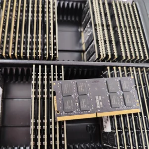
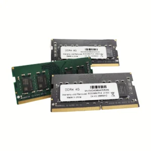
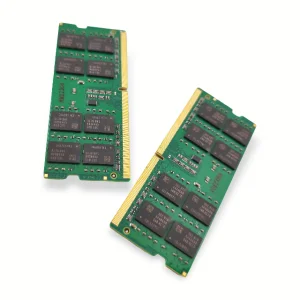
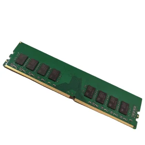
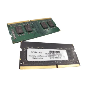
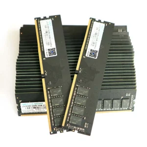
Integrating state-of-the-art DRAM subsystem manufacturing with precision circuit board production to serve global enterprises.
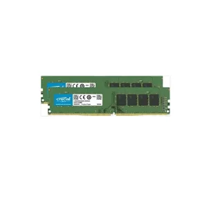
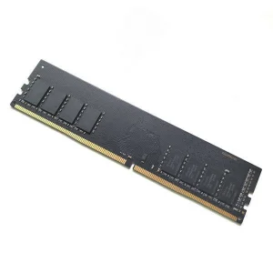
Founded in 2017, Memvora Electronics Technology Co., Ltd. is a professional manufacturer specializing in high-performance DDR5 memory modules, dedicated to delivering reliable memory solutions for consumer, industrial, enterprise, and embedded applications worldwide. With a modern manufacturing facility covering 386㎡, we combine advanced production equipment, strict quality management, and experienced engineering expertise to provide stable, high-speed memory products for global OEM and ODM partners.
Since entering the international market, Memvora has accumulated 7 years of export experience, serving customers across North America, Europe, Southeast Asia, the Middle East, and South America. Our annual export revenue exceeds US$18.6 million, supported by a strong global supply chain and long-term partnerships with more than 1,280 component suppliers and business partners.
With 14 years of industry experience, our team continuously invests in technology innovation and product development. Our R&D department consists of 126 professional engineers who focus on developing next-generation DDR5 memory solutions with higher speed, lower latency, and enhanced reliability. Last year alone, we successfully launched 86 new memory products to meet the evolving needs of gaming, AI computing, industrial automation, and enterprise servers.
Quality is the foundation of everything we do. Every product undergoes 100% functional testing, burn-in testing, compatibility testing, signal integrity testing, and aging tests before shipment. Our dedicated quality control team of 42 inspectors ensures every memory module meets rigorous international quality standards and delivers long-term stable performance.
Memvora provides flexible OEM, ODM, private label, custom capacity, PCB color, heat spreader design, firmware optimization, and packaging customization services to meet different market requirements. Backed by a responsive engineering team and efficient production management, we help customers shorten development cycles and accelerate product launches.
Today, Memvora serves a diverse customer base including memory brands, computer manufacturers, industrial equipment suppliers, system integrators, distributors, wholesalers, and e-commerce retailers. Through continuous innovation, reliable quality, and customer-focused service, we are committed to becoming a trusted global partner for advanced DDR5 memory manufacturing and customized DRAM solutions.
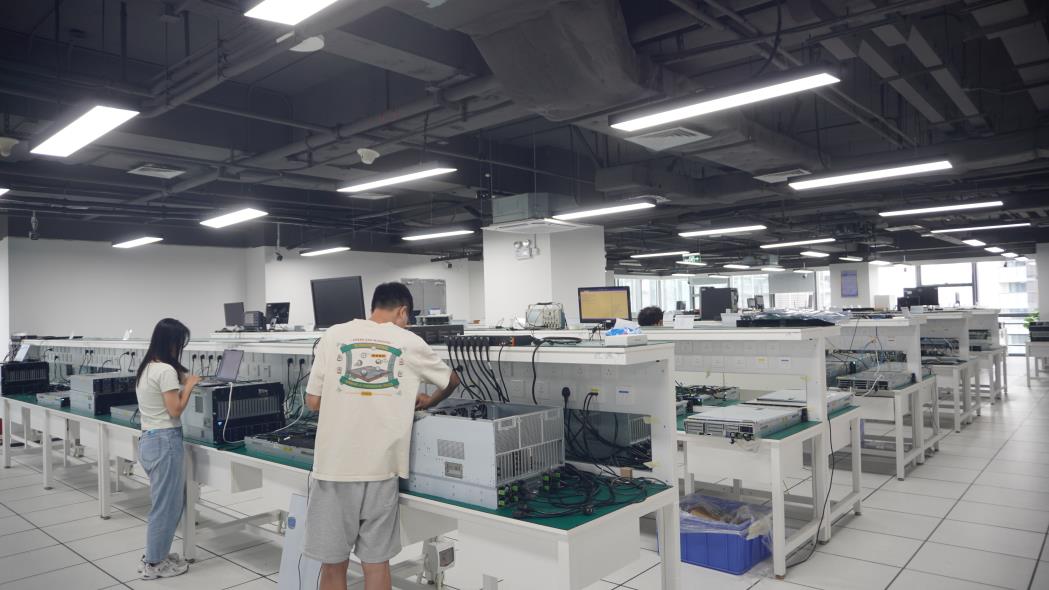
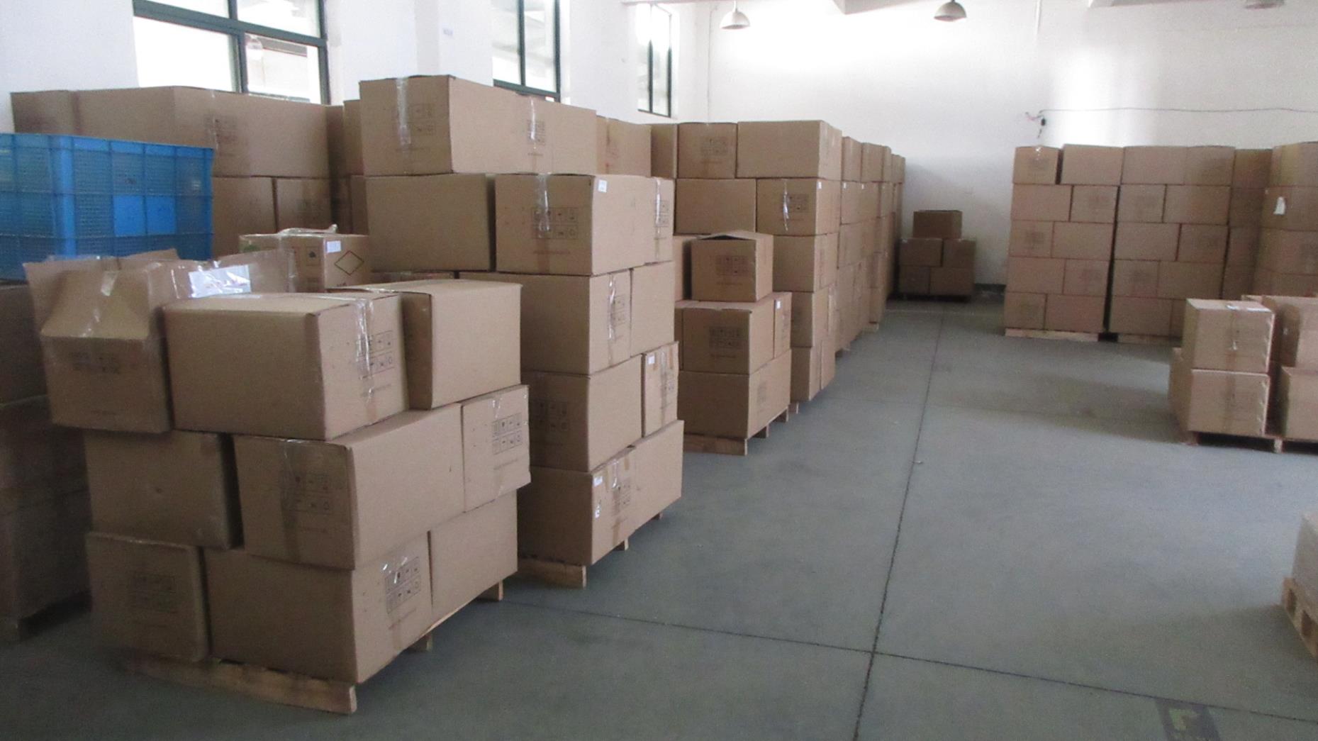
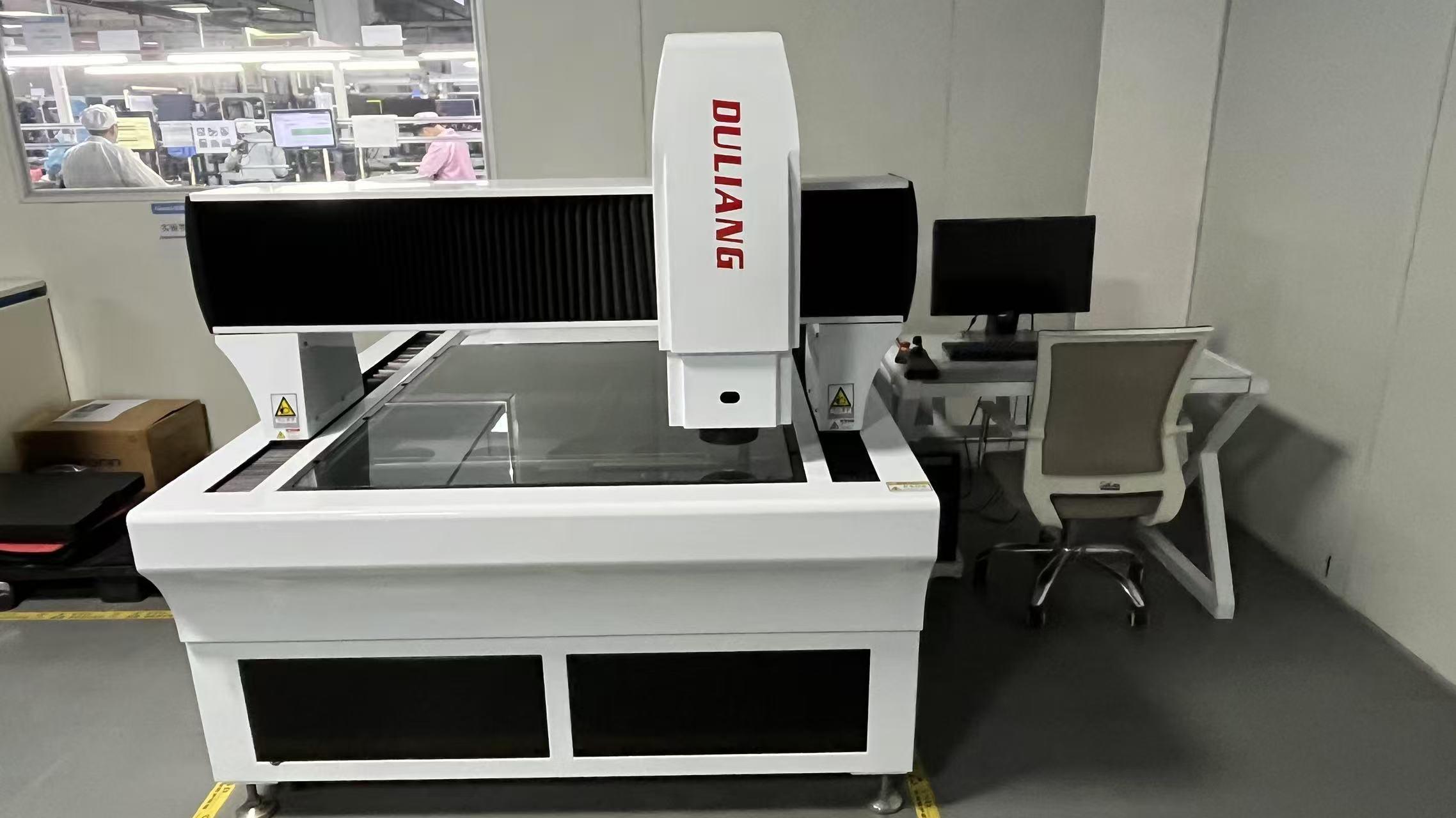
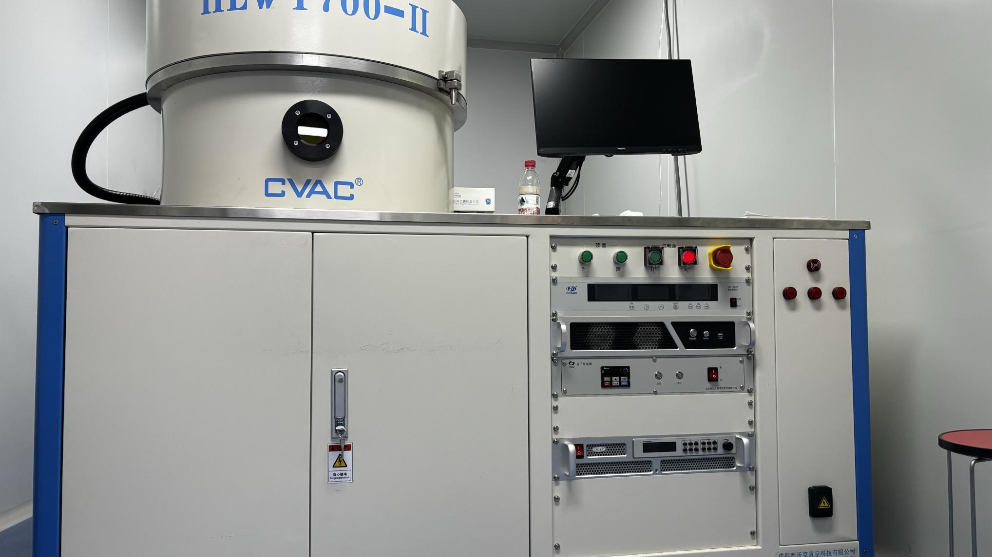
Take an inside look at our assembly lines, surface mount technology (SMT) stations, and heavy copper inspection zones.
Operating in critical industries requires rigorous compliance validation. Heavy copper boards must satisfy strict standards to ensure safety and reliability under electrical and thermal stress.
Every heavy copper circuit board and memory system is subjected to extensive testing protocols prior to shipping:
Technical questions about specifying, designing, and sourcing thick copper printed circuit boards.
Our comprehensive manufacturing lines support the following industry-grade products, built to withstand continuous processing and thermal stress.